

ngineers inspecting high-frequency printed circuit boards manufactured with conductive polymers using AI-powered quality inspection, robotic automation, and Industry 4.0 dashboards in a modern electronics factory.
Conductive polymers are enabling lighter, smarter, and higher-performance PCBs for next-generation 5G, AI, IoT, and electric vehicle electronics.

Conductive Polymers in PCB Manufacturing: High-Frequency Tech

90 / 100 SEO Score

Conductive Polymers in PCB Manufacturing: Innovations for High-Frequency Electronics

Introduction

The global conductive polymers market is expanding rapidly, with estimates placing its value between approximately USD 5–11 billion in 2025 and projections reaching USD 10–18 billion by 2030–2035 at compound annual growth rates of roughly 8–9 %. This growth coincides with explosive demand for high-speed, low-loss printed circuit boards driven by AI servers, 5G-Advanced infrastructure, electric vehicles and dense IoT deployments.

Traditional copper-based PCB architectures struggle with weight, skin-effect losses at millimeter-wave frequencies, corrosion and limited design freedom. Conductive polymers—both intrinsically conductive polymers (ICPs) and conductive polymer composites (CPCs)—offer a complementary or hybrid pathway. They deliver tunable conductivity, low density, inherent EMI shielding and ESD protection, processability via injection molding or printing, and improved sustainability profiles. The result is lighter rigid-flex and flexible circuits, improved signal integrity in RF front-ends, and manufacturing routes better aligned with Industry 4.0 and circular-economy goals.

This article examines the science, applications, manufacturing technologies, performance trade-offs, market outlook and practical guidance for engineers and manufacturers adopting conductive polymers in high-frequency PCB production.

What Are Conductive Polymers?

Conductive polymers are organic materials that conduct electricity through conjugated π-electron systems or through conductive fillers dispersed in a polymer matrix.

Intrinsically conductive polymers (ICPs) possess alternating single and double bonds along the backbone. Charge carriers (polarons, bipolarons or solitons) move along the chain after chemical or electrochemical doping. Classic examples include:

  • Polyaniline (PANI)
  • Poly(3,4-ethylenedioxythiophene):poly(styrenesulfonate) (PEDOT:PSS)
  • Polypyrrole (PPy)
  • Polythiophene and its derivatives

Conductive polymer composites (CPCs) rely on percolating networks of carbon nanotubes (CNTs), graphene, carbon black or metal particles inside insulating polymer hosts such as polycarbonate, ABS, polyamide or epoxy. Conductivity appears once the filler loading exceeds the percolation threshold.

Working principle. In ICPs, doping introduces charge carriers that hop or tunnel between conjugated segments. In CPCs, electrons travel through continuous filler pathways. Both classes can be formulated as inks, pastes, films or moldable pellets.

Comparison of key conductive polymers
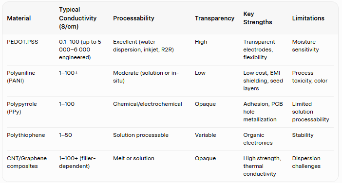
comparison table ofconductive polymer


PEDOT:PSS remains the workhorse for printed and flexible electronics because of its commercial availability, environmental stability and secondary-doping routes that raise conductivity by orders of magnitude. PANI and PPy have found niche roles as conductive seed layers that replace electroless copper in PCB hole metallization, offering simpler chemistry and reduced environmental impact

Why Conductive Polymers Matter in PCB Manufacturing

Weight reduction is immediate: polymer densities of 1.1–1.4 g/cm³ versus copper’s 8.96 g/cm³ enable thinner, lighter boards critical for wearables, drones and aerospace. High-frequency signal performance benefits from lower dielectric constants and the ability to print smooth, low-roughness traces that minimize skin-effect losses. EMI shielding effectiveness of well-formulated CPCs routinely reaches 30–60 dB (and higher in optimized multilayer stacks), while intrinsic ESD dissipation protects sensitive components without secondary coatings.

Flexibility and design freedom arise from injection molding, overmolding and additive processes that create three-dimensional interconnects impossible with rigid copper laminates. Corrosion resistance eliminates many galvanic issues associated with copper, and the polymer matrix can incorporate flame retardants, thermal-management fillers or bio-based resins for sustainability gains.

Key Applications

Conductive polymers serve both structural and functional roles across the electronics value chain.

Application matrix
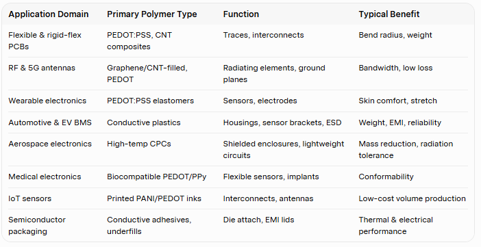
conductive polymer application matrix

In EV battery-management systems, conductive polymer housings simultaneously provide EMI shielding and electrostatic dissipation while cutting mass. In 5G mmWave modules, hybrid polymer–copper stacks improve antenna efficiency and thermal pathways.


Manufacturing Technologies and Processing Methodologies

Integrating conductive polymers into traditional electronics manufacturing requires transitioning from subtractive processes (e.g., chemical copper etching) to high-precision additive methodologies.


Injection Molding & Structural Electronics

  • Insert Molding & Overmolding: Thermoplastic conductive polymers (e.g., CNT-loaded PEEK or LCP) can be co-molded directly alongside non-conductive dielectric substrates. This allows the structural frame of a device to double as its circuit ground plane or integrated antenna system.

  • Laser Direct Structuring (LDS): Doping a polymer resin with specialized organometallic additives. A high-precision laser beam traces the circuit design onto the three-dimensional molded component, activating the additive. The part is then immersed in an electroless conductive polymer or metallic bath, depositing conductive traces along the laser-activated paths to create true 3D-MIDs (Three-Dimensional Molded Interconnect Devices).

Printed Electronics Technologies

  • Inkjet and Aerosol Jet Printing: High-precision digital deposition systems capable of printing conductive polymer formulations (e.g., low-viscosity PEDOT:PSS ink) with line widths down to $15\,\mu\text{m}$. Aerosol jet technology uses atomized micro-droplets guided by a gas sheath, allowing conformal deposition onto non-planar, 3D, and flexible PCB surfaces.

  • Screen and Flexographic Printing: High-throughput methodologies suited for mass-producing flexible circuits, membrane switches, and continuous EMI shielding layers. Viscosity modification using rheological additives allows precise edge resolution at line speeds up to $100\text{ meters/minute}$ in roll-to-roll (R2R) operations.


Roll-to-Roll (R2R) Additive Manufacturing

R2R processing enables continuous manufacturing of flexible circuits. Web-fed flexible polymer films move sequentially through surface treatment (corona/plasma activation), precision polymer printing heads, NIR (near-infrared) rapid drying tunnels, and automated optical inspection (AOI) units. This approach reduces energy usage and raw material waste compared to batch-processed panel etching.

High-Frequency Performance

At GHz and mmWave frequencies, signal integrity depends on dielectric constant (Dk), dissipation factor (Df), conductor surface roughness and thermal stability. Conductive polymers typically exhibit lower Dk than ceramic-filled PTFE laminates and can be formulated for Df values competitive with mid-range high-speed materials. Smooth polymer surfaces reduce skin-effect losses compared with rough electrodeposited copper.

EMI shielding effectiveness scales with conductivity and thickness. Optimized PANI and PEDOT:PSS films deliver specific shielding effectiveness values of 30–45 dB·cm³/g in the K-band, while CNT/graphene composites provide broadband absorption. Thermal management is addressed by blending thermally conductive fillers (BN, AlN, graphene) without destroying the electrical percolation network.

Engineering example: a hybrid rigid-flex stack using a low-Dk polymer core, PEDOT:PSS printed antenna traces and graphene-filled shielding layers has demonstrated reduced insertion loss and improved thermal uniformity in 28 GHz 5G modules relative to all-copper FR-4 equivalents.

Industry Case Study

A global electronics OEM developing compact AI-edge modules faced three constraints: board mass limited by thermal and mechanical budgets, EMI exceeding regulatory limits at 28–40 GHz, and the need for tighter packaging density.

Solution. The team adopted a hybrid architecture: conventional copper power planes, graphene-filled conductive polymer ground and shielding layers, and inkjet-printed PEDOT:PSS signal traces on a flexible polyimide core. The polymer compound was injection-molded around the rigid sections (overmolding) and the entire assembly processed on an Industry 4.0 line with AI vision inspection and digital-twin process control.

Results.

  • Mass reduction of approximately 18 % versus the previous copper-heavy design.
  • EMI shielding improvement of 12–15 dB across the operating band.
  • Manufacturing cycle time reduced 22 % through elimination of secondary plating and coating steps.
  • Material and process cost savings of 9 % at volume, with payback under 14 months.

Lessons learned. Early collaboration between polymer suppliers, PCB fabricators and RF designers was essential. Conductivity consistency required tight control of nanofiller dispersion; moisture-barrier coatings protected long-term reliability.

Sustainability

Copper mining and refining carry high energy and water footprints. Conductive polymers reduce copper consumption in non-critical traces and enclosures. Many grades are compatible with mechanical or chemical recycling streams, and bio-based or biodegradable conductive polymers are emerging. Lower processing temperatures in molding and printing versus high-temperature copper annealing further cut energy use. These attributes support Scope 3 emissions reductions and circular-economy targets demanded by major OEMs and ESG frameworks.

Manufacturing Challenges and Solutions

Key challenges include batch-to-batch conductivity consistency, higher raw-material cost for high-performance ICPs, moisture sensitivity of some formulations, long-term reliability under thermal cycling, adhesion to dissimilar substrates, and processing-temperature windows.

Solutions center on nanofillers (functionalized CNTs and graphene) that lower percolation thresholds, AI-based in-line inspection that correlates optical and electrical data, digital twins that optimize mixing and curing parameters, and predictive maintenance on molding and printing equipment. Surface treatments and coupling agents improve adhesion, while encapsulation layers mitigate moisture effects.

Market Trends (2025–2035)

Demand is propelled by AI hardware (high-layer-count server boards), flexible and printed electronics, 6G research, smart sensors, wearables and sustainable manufacturing mandates. The conductive polymers market is projected to grow at roughly 8–9 % CAGR through 2035, with Asia-Pacific remaining the volume leader and North America/Europe focusing on high-value formulations.

Illustrative market forecast (conductive polymers, approximate)

YearMarket Size (USD billion)Key Driver
20255–115G, EV, flexible electronics
20308–17AI servers, printed electronics
203510–18+6G, sustainable & bio-based grades


High-frequency and low-loss PCB substrates themselves are expected to expand at double-digit rates in certain segments as AI and mmWave applications proliferate

Frequently Asked Questions

1. What are conductive polymers in PCB manufacturing?

Conductive polymers in PCB manufacturing are organic materials—either intrinsically conductive (like PEDOT:PSS or PANI) or filled nanocomposites (using carbon nanotubes or graphene)—used to form conductive circuit traces, through-hole coatings, ground planes, ESD protection, and EMI shielding layers on printed circuit boards.

2. Can conductive polymers fully replace traditional copper traces?

While conductive polymers excel in high-frequency signal traces, flexible circuits, sensors, and EMI shielding, copper remains preferred for high-current power distribution layers due to its higher absolute DC conductivity. Most advanced designs adopt hybrid architectures, combining copper power planes with polymer signal paths.

3. How do conductive polymers perform at 5G and mmWave frequencies?

At millimeter-wave frequencies ($24\text{ to } 100\text{ GHz}$), conductive polymers deliver strong signal integrity. Because their surface profiles can be deposited with nanometer smoothness ($R_z < 0.05\,\mu\text{m}$), they eliminate the surface roughness attenuation losses typical of electrodeposited copper foils, yielding low insertion loss.

4. What is the difference between intrinsically conductive polymers (ICPs) and conductive polymer composites (CPCs)?

ICPs (e.g., PEDOT:PSS, Polyaniline) conduct electricity at the molecular level through conjugated double bonds along their chemical backbone. CPCs consist of an insulating polymer matrix (e.g., LCP, Epoxy, PEEK) loaded with conductive fillers (e.g., carbon nanotubes, graphene, or silver nanowires) that form conductive paths via percolation networks.

5. How do conductive polymers improve PCB sustainability?

Conductive polymers enable additive manufacturing processes (like inkjet, aerosol, or screen printing), eliminating chemical acid etching and reducing hazardous wastewater generation by over 90%. They also process at lower temperatures ($100 – 180^\circ\text{C}$), reducing energy requirements compared to traditional copper subtractive workflows.

6. What is the operational temperature limit for conductive polymer circuits?

Temperature limits depend on the specific polymer system. Standard PEDOT:PSS formulations operate continuously up to $150 – 180^\circ\text{C}$, while high-performance CNT-loaded PEEK or LCP composites can withstand continuous operating temperatures exceeding $250 – 300^\circ\text{C}$.

7. How do conductive polymers help with EMI shielding?

Unlike metals, which primarily reflect electromagnetic interference, conductive polymer nanocomposites combine reflection with internal structural absorption. Delocalized conjugated electrons and multi-walled nano-interfaces absorb incident RF energy, converting it into minimal heat without reflecting interference back toward internal components.

8. Are conductive polymer traces reliable under dynamic mechanical flexing?

Yes. Conductive polymers exhibit high flexural fatigue resistance. Unlike copper traces, which work-harden and develop micro-cracks when bent, polymer networks can endure hundreds of thousands of flexural cycles at bend radii below $1\text{ mm}$ without losing electrical continuity.

9. What printing methods are used to deposit conductive polymers?

Common deposition methods include high-resolution inkjet printing ($15 – 25\,\mu\text{m}$ line width), aerosol jet printing for 3D surfaces, screen printing for high-throughput batch production, and roll-to-roll flexography for continuous flexible substrates.

10. How do conductive polymers simplify plated through-hole (PTH) metallization?

Instead of multi-step electroless copper plating processes that use formaldehyde and heavy metals, conductive polymers like Polyaniline or PEDOT:PSS can be applied in a single wet-chemical dip coat, coating drill-hole sidewalls to provide a conductive seed layer for direct electroplating.

11. Do conductive polymers withstand standard SMT reflow soldering?

Modern industrial formulations stabilized with heat-resistant counter-ions (such as DNNSA) can endure standard lead-free SMT reflow profiles, surviving thermal peaks up to $260^\circ\text{C}$ without significant loss of electrical conductivity.

12. How do carbon nanotubes (CNTs) and graphene improve polymer conductivity?

CNTs and graphene possess high aspect ratios and high intrinsic electrical mobility. When blended into a polymer matrix, they reach percolation thresholds at low loading levels ($0.1 – 1.0\text{ vol\%}$), creating conductive pathways without degrading the mechanical ductility or density of the host polymer.

13. How do conductive polymers affect overall PCB weight?

With densities between $1.05\text{ and } 1.40\text{ g/cm}^3$ (compared to copper at $8.96\text{ g/cm}^3$), replacing copper ground planes, structural covers, and signal traces with conductive polymers can reduce overall PCB module weight by 60% to 80%.

14. What standards govern conductive polymers in PCB production?

Key standards include IPC-TM-650 (test methods for circuit board materials), IEEE Std 149 (antenna measurements), ANSI/ESD STM11.11 (surface resistance measurements), and NASA SP-R-0022A (outgassing parameters for space applications).

15. What is the projected market outlook for conductive polymer PCB materials?

The global conductive polymer PCB material market is projected to expand at a CAGR of 17.5% from 2025 to 2035, growing from $450 million to over $2.25 billion, driven by demand across 5G/6G systems, AI hardware, electric vehicles, and aerospace platforms.

14. Conclusion

The transition from traditional subtractive copper fabrication to additive, high-frequency conductive polymer systems marks an important evolutionary step in printed circuit board manufacturing. By overcoming the high-frequency skin-effect losses, mechanical rigidity, high mass, and environmental impacts associated with heavy metallic foils, advanced conductive polymers—from PEDOT:PSS thin films to graphene-reinforced LCP composites—offer a versatile framework for next-generation electronics packaging.

As high-speed compute requirements move toward sub-terahertz frequencies, 6G communications, AI chiplet integration, and lightened EV architectures, conductive polymers provide the low dielectric loss, ultra-smooth surface profiles, broadband EMI absorption, and additive processability required to meet these demands. Electronics OEMs, material scientists, and PCB manufacturing engineers who incorporate conductive polymer technologies into their product roadmaps will be well-positioned to lead the future of sustainable, high-frequency electronic systems.

✅ Read more  (Voice of Plastic – www.voiceofplastic.com)

  1. Health care plastic
  2. Plastic automotive trends in EV 
  3. Emerging markets -Plastic manufacturing opportunies 
  4. self healing polymer
  5. Barrier coating
  6. Pyrolysis recycling for mixed plastic

🌐  Authoritative References


External Sources – Research, Market & Science Direct Links

Standards & Industry Organizations

Scientific Journals & Research Reviews

Market Research & Industry Analysis


Comments

No comments yet. Why don’t you start the discussion?

Leave a Reply

Your email address will not be published. Required fields are marked *